One of the most versatile linear integrated circuit is 555 timer. 555 timer IC was first introduced in early 1970 by Signetics Corporation.555 timer IC is incredibly low cost and popular timing IC that is used by electronics student, hobbyist for generating timing delay and pulses. Mono stabale and astable multi vibrators is that the most correct example of its application. With the exception of this it's conjointly used for oscillations, waveform generators, analog frequency meters, voltage regulators, digital probes, tone generation, frequency divider and lots of others.This device is obtainable as 8-pin mini Dual-in-line package(DIP) or 14 pin Dual-in-line package(DIP) that consist 25 transistor,16 resistors, 2 diode.
Pin 1: Ground This pin is used to measured the all voltages.
Pin 2: Trigger Negative going pulse is applied to this pin whose dc level is greater than 1/3 times VCC. Thus comparator 2 output goes low. The output remains high as long as trigger terminal is held at low voltage.
Pin 3: Output Output pin is available to connect the load.There are two ways of connecting the load either between pin 3 and ground or between pin 3 and +Vcc pin of 555 timer IC.
Pin 4: Reset 555 timer can be reset by applying a negative pulse to this pin.
Pin 5: control voltage To change the threshold voltage and trigger voltage an external voltage is applied to this pin.
Pin 6: Threshold SR flip flop is reset when voltage at this pin is greater than 2/3 Vcc.
Pin 7: Discharge This pin is directly connected to the collector of transistor.When transistor is off this acts as a open circuit and when transistor is on, acts as a shot circuit.
Pin 8: A Supply voltage is applied to this pin that ranges from +5v to +18v with respect to the ground.
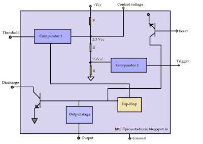
Block Diagram of 555 Timer IC
555 Timer IC has three operative modes known as:
1: Monostable
2: Astable
3: Bistable
To Know additional concerning 555 IC Click on this 555 Data sheet.
PIN CONFIGURATION OF 555 TIMER IC
 |
| 8-Pin DIP 555 Timer IC |
Pin 1: Ground This pin is used to measured the all voltages.
Pin 2: Trigger Negative going pulse is applied to this pin whose dc level is greater than 1/3 times VCC. Thus comparator 2 output goes low. The output remains high as long as trigger terminal is held at low voltage.
Pin 3: Output Output pin is available to connect the load.There are two ways of connecting the load either between pin 3 and ground or between pin 3 and +Vcc pin of 555 timer IC.
Pin 4: Reset 555 timer can be reset by applying a negative pulse to this pin.
Pin 5: control voltage To change the threshold voltage and trigger voltage an external voltage is applied to this pin.
Pin 6: Threshold SR flip flop is reset when voltage at this pin is greater than 2/3 Vcc.
Pin 7: Discharge This pin is directly connected to the collector of transistor.When transistor is off this acts as a open circuit and when transistor is on, acts as a shot circuit.
Pin 8: A Supply voltage is applied to this pin that ranges from +5v to +18v with respect to the ground.
Block Diagram of 555 Timer IC
 |
| 555 Timer IC Block Diagram |
The 555 timer IC work as a mono-stable multi-vibrator and astable multi-vibrator. A voltage divider circuit is internally connected to the Pin 8 and Pin 1 of 555 timer IC. This circuit hold positive non inverting terminal of comparator at 1/3Vcc and negative inverting terminal of comparator at 2/3Vcc. The output from each comparator is connected to the input of the SR Flip-Flop. The output from the SR Flip-flop acts as a switching stage to drive the Load.
555 Timer IC has three operative modes known as:
1: Monostable
2: Astable
3: Bistable
To Know additional concerning 555 IC Click on this 555 Data sheet.

0 comments:
Post a Comment